Weighing Attograms
January 27, 2014
One thing that
materials scientists do often is the fabrication of thin
films of materials on other materials.
Metal layers are often required for
electrical connection, and sometimes the metals themselves are useful for sensors such as
thermocouples. Evaporation is the most common technique for making films of pure metals, while
alloys generally need the more advanced technique of
sputtering.
You usually want to produce a layer of a certain thickness. One way to do this for evaporation is to evaporate a fixed quantity of material placed a known distance from your
substrate. The metal will evaporate in a
spherical front, so it's easy to calculate the final
areal density of material produced at the distance of your substrate.
Sometimes you need to know the thickness to better accuracy, and that's when
film thickness monitors are used. These
typically employ quartz crystal resonators that are placed the same distance from the metal source as your substrate.
Mass loading of the crystal decreases its
oscillation frequency, and the frequency change will indicate the thickness of deposited layer.
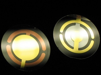
Quartz crystal resonators for film thickness monitoring.
The front and back electrodes connect to electronic oscillator circuitry.
(Via Wikimedia Commons.)
The quartz crystals for such monitors are inexpensive. This is a good thing, since the crystals will become less accurate as mass is deposited, and they will stop oscillation when they're too loaded. In practice, the crystals are replaced long before they stop oscillation, since this operating regime is well past the limit for
accurate measurement.
Commercial monitors are available, and these will display thickness directly when you preset the material
density; but a simple
oscillator,
frequency counter and a
calculator are all you need. The
circuitry is easy to build for someone knowledgeable in
electronics, and a former
colleague of mine published a circuit with
nanometer resolution.[1]
As material is deposited on the resonator crystal, its resonant frequency will decrease according to the
Sauerbrey equation, an equation derived by
German physicist, Günter Sauerbrey,[2]
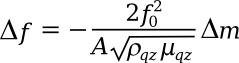
in which
Δf is the frequency change in
hertz,
f0 is the initial frequency in hertz,
A is the
area of the resonant portion of the crystal,
ρqz is the crystal density (2.648
g/cc for quartz),
μqz is the
shear modulus of the crystal (2.947 x 10
11 g/cm-s2 for AT-cut quartz), and
ΔM is the mass change in
grams. It's assumed that the mass loading is small, corresponding to a frequency change of less than 2%.
The crystals for this application are large, about an
inch in
diameter, and they resonate at a few tens of
MHz at most. If you intend to weigh smaller bits of material, a resonant
cantilever is a better approach. I wrote about cantilevers for
vibration energy-harvesting applications in a
previous article (Energy Harvesting Cantilevers, January 14, 2013).
The cantilever, clamped at one end as shown in the figure, is one of the more interesting mechanical objects. It's well known to mechanical engineers, since its properties are explained by some simple mathematics.
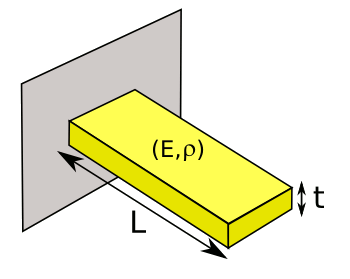
A cantilever beam.
(Illustration by the author, rendered using Inkscape.)
The resonant frequency of such a cantilever is given as
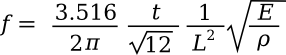
where t is the beam thickness, L is the beam length, E is Young's modulus, and ρ is the material density. Surprisingly, the width of the beam doesn't figure into the formula. I've written a spreadsheet (available here) for calculation of cantilever resonance frequency.
It depends on where the mass (m) is added, but adding mass to a cantilever changes the resonance frequency changes in proportion to m-1/2. Using MEMS techniques, it's possible to make small, silicon cantilever resonators with a mass sensitivity exceeding 10-18 grams; that is, an attogram, which is about the weight of individual large protein molecules.[3]
The resonance of such MEMS cantilevers is achieved by using electrostatic drive from nearby electrodes. Such cantilevers have a typical thickness of about micrometer and a length of a few tens to a hundred micrometers. This yields a resonant frequency in the low MHz range. Having a low resonance frequency is a disadvantage, since it makes sensing frequency change more difficult.
The most common application for MEMS cantilevers is chemical and biological sensing. An immunosensor is simply made by putting an antibody layer on a cantilever. The antibody will selectively absorb the target analyte to allow detection. One problem is that resonance is damped when the cantilever is placed in a liquid.
The problems associated with using cantilever sensors in liquids have been solved by a research team of scientists from MIT, Innovative Micro Technology (Santa Barbara, CA), Sogang University (Seoul, Korea), and the Howard Hughes Medical Institute (Cambridge, MA). They made a sensor with an inverse topology that has the liquid on the inside instead of the outside. The liquid flows though a microchannel bonded to the cantilever, as shown in the figure.[5-7]
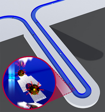
A suspended nanochannel resonator (SNR) capable of weighing individual nanoparticles with attogram precision.
The inset illustrates the interior of the microfluidic channel where DNA-coated gold nanoparticles are flowing.
(MIT image by Selim Olcum and Nate Cermak.)
Their sensor, called a suspended microchannel resonator (SMR), is capable of measuring the mass of individual 10 nm particles with 0.85 attogram precision.[5] This sensitivity approaches the thermomechanical noise limit, and the sensor is capable of measuring more than 18,000 particles in an hour.[5-6] The cantilever is 22.5 micrometers in length, with a channel that's a micrometer wide and 0.4 micrometers deep.
Such a small cantilever has a high resonance frequency, so the device is more sensitive. Cantilever excitation is piezoelectric, rather than electrostatic.[6] Says Selim Olcum, an MIT postdoc and a lead author of the paper describing this work,
"Now we can weigh small viruses, extracellular vesicles, and most of the engineered nanoparticles that are being used for nanomedicine."[6]
This sensor is an improved version of a device developed by MIT in 2007.[7] That device had femtogram resolution. This sensor has application for detecting exosomes, blood proteins associated with Glioblastoma multiforme, a common and malignant brain tumor in humans.[6] It can also measure the size distribution of nanoparticles.[7]
This research was funded by the U.S. Army Research Office, the National Science Foundation, and the National Cancer Institute.[6]
References:
- H. A. Ashworth and L. W. Shacklette, "Mass/thickness detector employing inexpensive integrated circuits," Rev. Sci. Instrum., vol. 49, no. 12 (December 1978), pp. 1653-1657.
- Günter Sauerbrey, "Verwendung von Schwingquarzen zur Wägung dünner Schichten und zur Mikrowägung," Zeitschrift für Physik, vol. 155, no. 2 (April 1959), pp. 206-222.
- G. Abadal, Z. J. Davis, B. Helbo, X Borrisé, R Ruiz, A Boisen, F Campabadal, J Esteve, E Figueras, F Pérez-Murano and N Barniol, "Electromechanical model of a resonating nano-cantilever-based sensor for high-resolution and high-sensitivity mass detection," Nanotechnology, vol. 12, no. 2 (June, 2001), pp. 85-186. A PDF copy is available, here.
- Ram Datar, Seonghwan Kim, Sangmin Jeon, Peter Hesketh, Scott Manalis, Anja Boisen and Thomas Thundat, "Cantilever Sensors: Nanomechanical
Tools for Diagnostics," MRS Bulletin, vol. 34 (June, 2009), pp. 449-454 (PDF File).
- Selim Olcum, Nathan Cermak, Steven C. Wasserman, Kathleen S. Christine, Hiroshi Atsumi, Kris R. Payer, Wenjiang Shen, Jungchul Lee, Angela M. Belcher, Sangeeta N. Bhatia and Scott R. Manalis, "Weighing nanoparticles in solution at the attogram scale," Proc. Natl. Acad. Sci., Early Edition, January 13, 2014, doi: 10.1073/pnas.1318602111.
- Anne Trafton, "Weighing particles at the attogram scale," MIT Press Release, January 13, 2014.
- Anne Trafton, "New MIT technique weighs single living cells," MIT Press Release, April 25, 2007.
Permanent Link to this article
Linked Keywords: Materials science; materials scientist; coating; film; metal; electrical conductor; electrical connection; thermocouple; evaporation; alloy; sputtering; substrate; sphere; spherical; areal density; film thickness monitor; quartz crystal microbalance; quartz crystal; resonator; mass; oscillation; frequency; electrode; electronic oscillator circuitry; Wikimedia Commons; accuracy and precision; density; oscillator; frequency counter; calculator; electronic circuit; circuitry; electronics; collegiality; colleague; nanometer; Sauerbrey equation; German; physicist; hertz; area; kilogram per cubic meter; g/cc; shear modulus; pascal; g/cm-s2; gram; inch; diameter; MHz; cantilever; vibration; energy-harvesting; mechanics; mechanical; mechanical engineering; mechanical engineer; mathematics; Inkscape; Young's modulus; density; spreadsheet; microelectromechanical systems; MEMS; silicon; attogram; protein molecule; Coulomb's law; electrostatic; micrometer; chemical compound; biology; biological; sensor; sensing; immunosensor; antibody; analyte; damping; damped; liquid; research; scientist; Massachusetts Institute of Technology; MIT; Innovative Micro Technology (Santa Barbara, CA); Sogang University (Seoul, Korea); Howard Hughes Medical Institute (Cambridge, MA); topology; microchannel; nanoparticle; precision; DNA; gold; Selim Olcum; Nate Cermak; nanometer; nm; phonon noise; thermomechanical noise; piezoelectricity; piezoelectric; postdoctoral research; postdoc; scientific literature; virus; extracellular vesicle; nanomedicine; femtogram; exosome; Glioblastoma multiforme; U.S. Army Research Office; National Science Foundation; National Cancer Institute.