Crystals without Facets
November 7, 2014
I was born and raised in
Upstate New York, about fifteen
miles from
Herkimer, New York, a
village with a
population of less than 10,000 people. One
summer, I tended to the
transmitter of a small
AM radio station there while its
chief engineer was on
vacation.
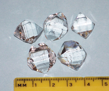
The
Herkimer area is famous for
Herkimer diamonds. These are large, clear
crystals found in
dolomite rock, and they aren't really
diamonds. They're
quartz, the
crystalline form of
silicon dioxide (silica, SiO
2), and they're impressive since they are large and
double-terminated; that is, they exhibit
facets all around.
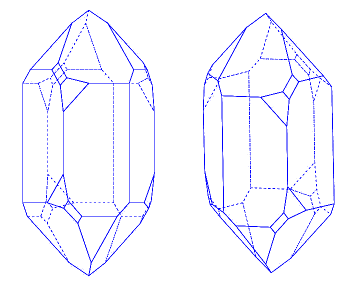
Crystal facets of quartz.
Quartz grows as left- and right-handed crystals, as shown.
(Left image and right image by "strickja," via Via Wikimedia Commons, modified.)
Herkimer crystals were formed in
nature by
hydrothermal crystallization in which silica, dissolved in hot
water, is transported to a
seed crystal to allow the crystal to grow to a larger size. The principal use of quartz crystals for the last
century was as the
frequency-determining element in
radio circuits, followed by its use in such things as
digital watches and
computers. Natural quartz was mined for this purpose until
World War II made the usual supply sources inaccessible.
industrial synthesis of quartz was developed at
Bell Labs by A. C. Walker;[1] and by Ernie Buehler,[2] with whom I worked for several years.
Crystals form in regular shapes, since the
attractive forces of their constituent
atoms or
molecules, as constrained by the
lowest energy packing arrangement, allow just certain combinations. These shapes can be as simple as a
cube, as found in
table salt and
iron crystals; or, much more complex, as shown in quartz crystals. Crystals demonstrate facets, since the rate of growth for the crystal is different for different
crystal planes because of
surface energy effects.
Synthetic Berlinite (AlPO4), crystals grown by hydrothermal synthesis.[3] The small divisions on the ruler are millimeters.
This material is isostructural with quartz.
(Photo by the author, as uploaded to Wikimedia Commons.)
Facet-free crystals are occasionally found in nature, but not in
laboratory synthesis. The usual product is either an
amorphous film, or faceted crystallites. That's why it's significant that
engineers and
physicists from the
University of Michigan (Ann Arbor, Michigan) have found a way to routinely produce rounded, facet-free,
nanoscale crystals of
boron subphthalocyanine chloride, an
organic solar cell material.[4-7]
The process produces a crystalline layer with a
lobe texture like that of
starfish shells (see figure). Says
Olga Shalev, a
doctoral student in
materials science and engineering at the University of Michigan and lead member of the
research team, "We call them nanolobes. They look like little
hot air balloons that are rising from the surface."[6]
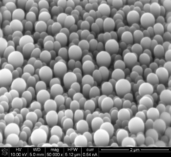
Micrograph of the non-faceted texture of a boron subphthalocyanine chloride layer.
(Image: University of Michigan/Max Shtein.)
Echinoderms, such as starfish, display similar rounded structures on their bodies that act as
lenses for their primitive
eyes. As
Max Shtein, a University of Michigan
associate professor in several departments, including materials science and engineering, comments,
"In my years of working with these kinds of materials, I've never seen shapes that looked like these. They're reminiscent of what you get from biological processes... Nature can sometimes produce crystals that are smooth, but engineers haven't been able to do it reliably."[6]
Boron subphthalocyanine chloride, from which these layers are made, is a small molecule that makes either flat films or faceted crystals with sharp edges. Once again,
serendipity advanced
science when
Shaurjo Biswas, a doctoral student at the University of Michigan in 2010, was using organic vapor jet printing to make solar cells from this material. He found that layers of thickness greater than about 600
nm exhibited a texture, so he decided to make thicker films. The nanolobe pattern emerged at a thickness of 800 nm.[6]
After a while, Shalev continued production and
analysis of these layers, systematically varying the growth conditions in an improved
apparatus. Eventually, others joined the research effort that culminated in a
paper in a recent issue of
Nature Communications.[6] Shtein had helped to develop the organic vapor jet printing process as a
graduate student. It's essentially like
spray painting, but with a
gas instead of a
liquid, and it has the advantage that the process doesn't require a
vacuum.[4,6]
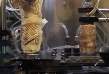
Portion of the organic vapor jet printing apparatus.
This photo conveys no useful information, but I always enjoy looking at laboratory apparatus.
(Still image from a YouTube video.)[7)]
One possible application is textured surfaces with controlled
wettability,
technologies for which
surface area films are desired, and
nonreflective coatings.[4,6] This research was funded by the
U.S. Department of Energy,
Office of Basic Energy Sciences, the
National Science Foundation, and the
Air Force Office of Scientific Research.[6]
References:
- A. C. Walker, "Hydrothermal Synthesis of Quartz Crystals," Journal of the American Ceramic Society, vol. 36, no. 8 (August, 1953), pp. 250-256.
- Ernest Buehler, "Method of growing quartz crystals," US Patent No. 2,785,058, March 12, 1957.
- Bruce H. Chai, Ernest Buehler, and John J. Flynn, "Alpha aluminum- or alpha gallium- orthophosphate crystals, wafers for acoustic wave devices," US Patent No. 4,559,208, December 17, 1985.
- O. Shalev, S. Biswas, Y. Yang, T. Eddir, W. Lu, R. Clarke, and M. Shtein, "Growth and modelling of spherical crystalline morphologies of molecular materials," Nature Communications, vol. 5, article no. 5204 (October 16, 2014), doi:10.1038/ncomms6204.
- Supplementary information for ref. 4 (PDF File).
- Nicole Casal Moore, "Facetless crystals that mimic starfish shells could advance 3D-printing pills," University of Michigan Press Release, October 20, 2014.
- Nanolobes, YouTube video by Michigan Engineering, October 16, 2014.
Permanent Link to this article
Linked Keywords: Upstate New York; mile; Herkimer, New York; village; population; summer; transmitter; AM radio station; broadcast engineering; chief engineer; vacation; Herkimer County, New York; Herkimer diamond; crystal; dolomite rock; diamond; quartz; crystalline; silicon dioxide; double terminated crystal; double-terminated; facet; chirality; left- and right-handed; Wikimedia Commons; nature; hydrothermal synthesis; hydrothermal crystallization; water; seed crystal; century; frequency; radio; electronic circuit; digital watch; computer; World War II; industry; industrial; chemical synthesis; Bell Labs; Coulomb's law; attractive force; atom; molecule; thermodynamic free energy; relative density; packing; cube; sodium chloride; table salt; iron; crystal plane; surface energy; synthetic and artificial gemstones; Berlinite; millimeter; laboratory; amorphous solid; engineer; physicist; University of Michigan (Ann Arbor, Michigan); nanoscopic scale; nanoscale; boron; phthalocyanine; chloride; organic compound; solar cell; material; lobe; starfish; seashell; shell; Olga Shalev; doctoral student; materials science and engineering; research; hot air balloon; electron microscope; micrograph; Max Shtein; Echinoderm; lens; eye; associate professor; serendipity; science; Shaurjo Biswas; nanometer; nm; analysis; laboratory equipment; apparatus; scientific literature; paper; Nature Communications; postgraduate education; graduate student; spray painting; gas; liquid; vacuum; YouTube video; wetting; wettability; technology; technologies; surface area; anti-reflective coating; nonreflective coating; U.S. Department of Energy; Office of Basic Energy Sciences; National Science Foundation; Air Force Office of Scientific Research; Ernest Buehler, "Method of growing quartz crystals," US Patent No. 2,785,058, March 12, 1957; Bruce H. Chai, Ernest Buehler, and John J. Flynn, "Alpha aluminum- or alpha gallium- orthophosphate crystals, wafers for acoustic wave devices," US Patent No. 4,559,208, December 17, 1985.